EXCELLENT THERMAL MANAGEMENT
High thermal conductivity for efficient heat dissipation
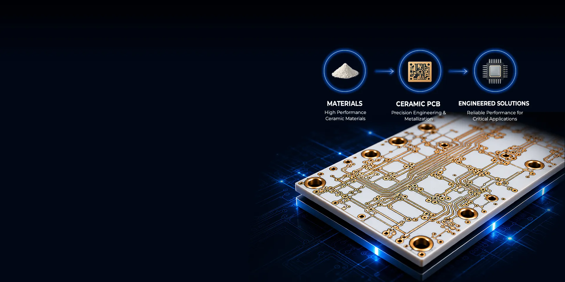
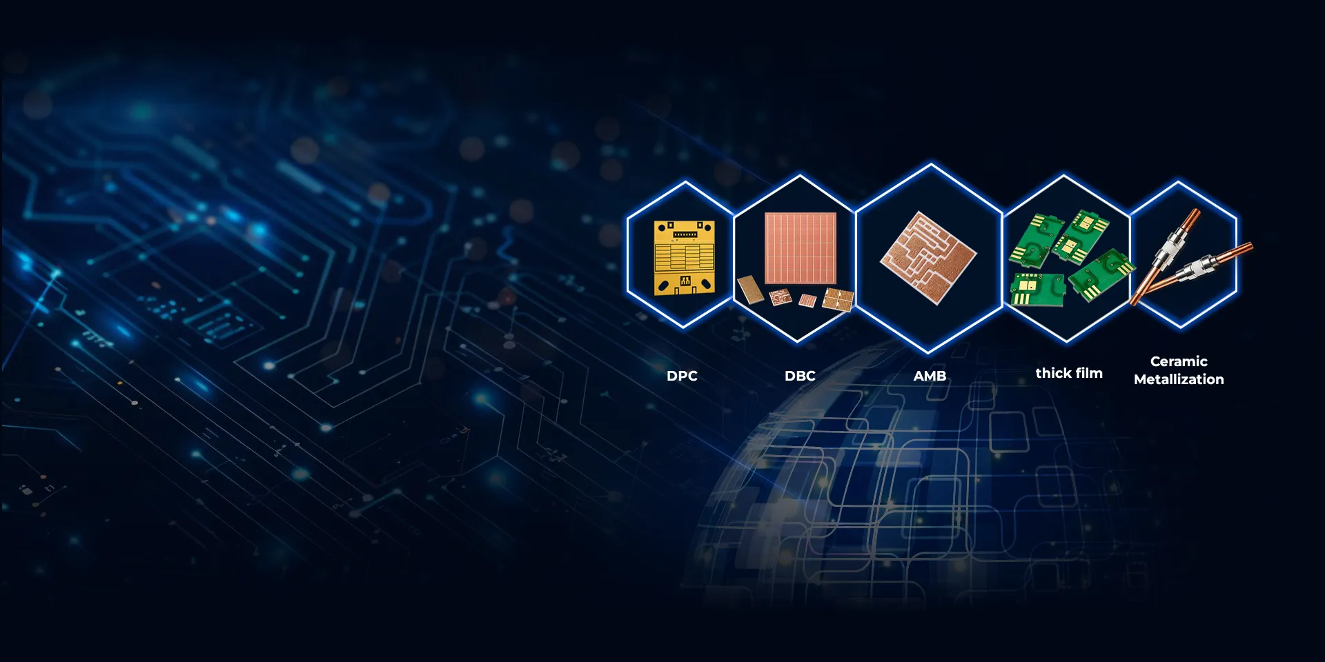

High thermal conductivity for efficient heat dissipation

Superior dielectric properties ensure electrical reliability

Stable performance in harsh environments

Enabling smaller size and higher power output
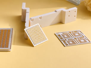
Fine-line ceramic substrates for semiconductor and RF applications
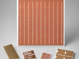
High current and high power ceramic solutions for EV and industrial power electronics
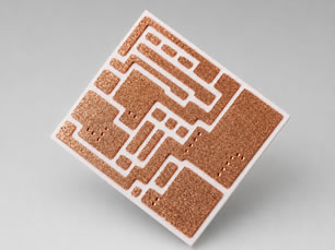
Enhanced reliability ceramic substrates for harsh operating environments
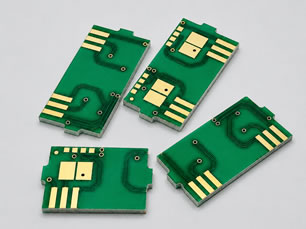
Cost-effective ceramic circuitry for hybrid electronics
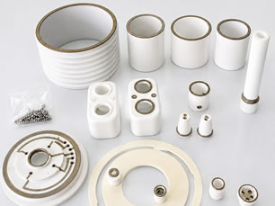
Custom ceramic-to-metal assemblies and vacuum brazing solutions





High thermal conductivity up to 170 W/mK
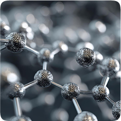
Cost-effective solution with excellent electrical insulation
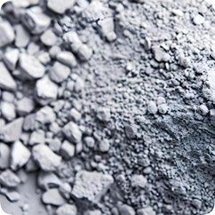
Exceptional mechanical strength and thermal shock resistance

Application-oriented technical support

Access to qualified global manufacturing resources

Material selection and design optimization support

Rapid sampling and pilot production support

Serving customers in Europe, North America and Japan

Effective supply chain management and on-time delivery

Compare AlN, Al₂O₃, and Si₃N₄ ceramic substrates based on thermal performance, mechanical strength, reliability, and applications.

Compare Ceramic PCB and FR4 to find the right substrate for thermal performance, reliability, and application requirements.

Compare DPC, DBC, and AMB technologies to understand their processes, advantages, and suitable applications.
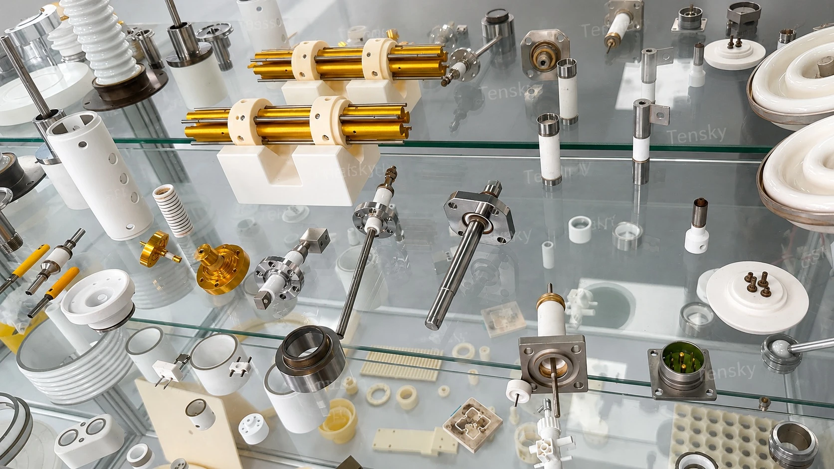
A brazing technology that creates strong, reliable, and hermetic ceramic-to-metal joints.